Taylored Bottum-Up Nanostructures
Using the methodology of atom manipulation we can assemble, one atomic spin at a time, magnetic nanostructures on metallic surfaces of almost any conceivable shapes and magnetic couplings. Changing the separations of the atomic spins within the nanostructure, their mutual coupling strengths and signs (ferromagnetic or antiferromagnetic) are tailored by exploring Ruderman-Kittel-Kasuya-Yosida (RKKY) exchange. We have studied various magnetic nanostructures like chains and arrays. Even working model systems of atomic spintronic devices as logic gates have been built.
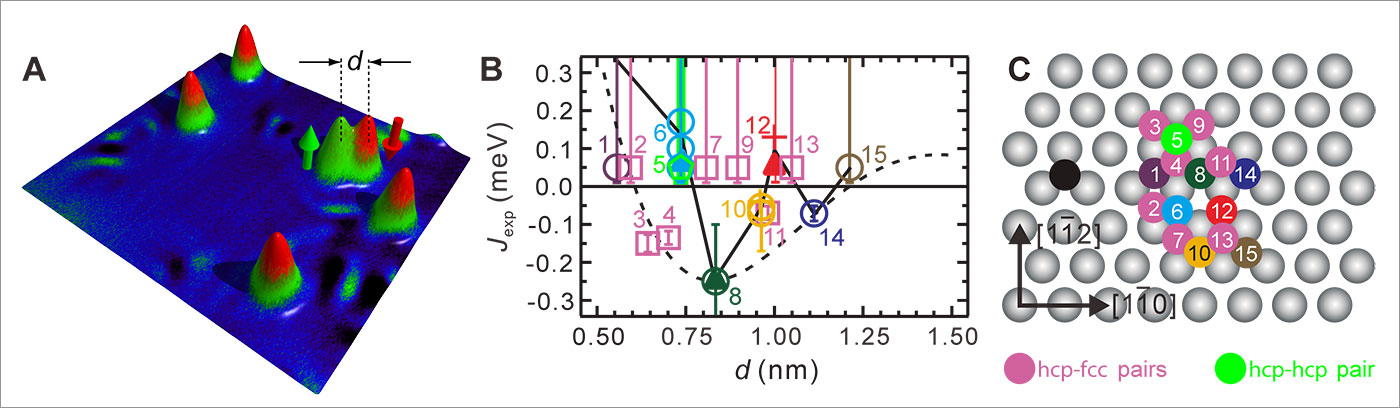
Fig.1: Ruderman-Kittel-Kasuya-Yosida (RKKY) interaction is a magnetic coupling between atomic spins doped into metallic hosts mediated by the oscillatory spin-polarization of the itinerant host conduction electrons which screen a local spin. As a consequence the interaction (Jexp) oscillates between ferromagnetic (Jexp>0) and antiferromagnetic (Jexp0) as a function of the separation (d) of the two atomic spins (see spin-resolved image A). Using single-atom magnetometry we have directly measured roadmaps of Jexp (see image B) in pairs of atomic spins as a function of their relative separation and orientation on the substrate lattice (see image C). RKKY interaction dominates the other magnetic interactions, direct and dipolar exchange, for distances of a few lattice constants and is ideally suited to tailor the couplings in dilute magnetic nanostructures.
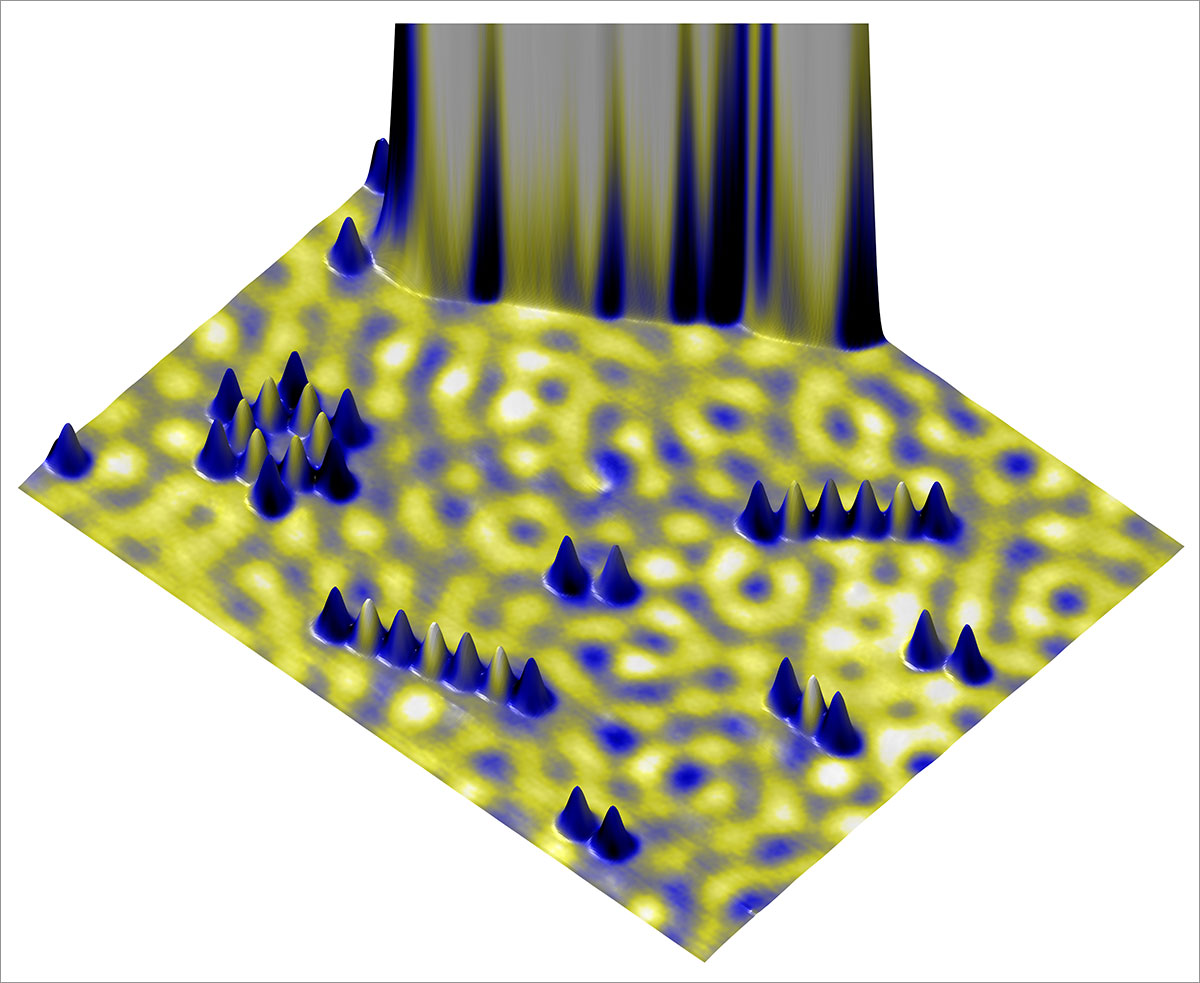 Fig.2: Using the experimentally determined roadmaps of RKKY interaction, we can tailor dilute nanomagnets of arbitrary shapes and internal couplings. For illustration, the spin-resolved image shows a part of an antiferromagnetic Kagome lattice and antiferromagnetic chains of three, six and seven atoms assembled from iron atoms on the (111) surface of copper. A cobalt island is visible in the left upper corner. We study the magnetic properties of such nanomagnets by single-atom magnetometry.
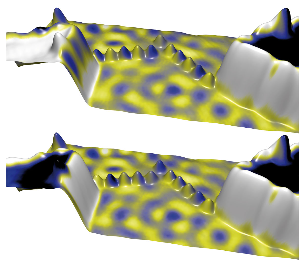
Fig.3: For proof of principles of novel atomic spintronics concepts, we have built working model systems of logic devices. The figure illustrates spin-resolved images of two input configurations of an OR gate built from two cobalt islands (triangular hills), and eleven iron atoms (hillocks) assembled on the (111) surface of copper. Devices that use such atomic spintronic concepts are envisioned to be smaller and faster, and have lower energy consumption than conventional silicon CMOS technology.