Atomic Spins
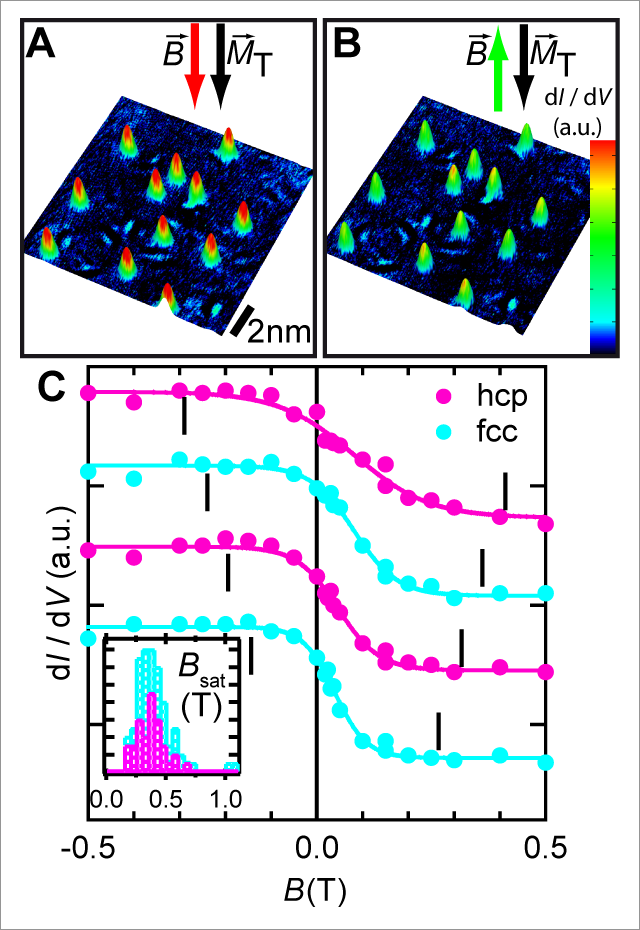 Fig.1: Using Single Atom Magnetometry we are able to map the magnetization of single atomic spins on different solid state surfaces as a function of an applied magnetic field (images A,B). The resulting magnetization curves (image C) of each individual atomic spin within the area of the spin-resolved images can be analysed with respect to their magnetic moments, anisotropies and interactions. We typically find broad variations of these magnetic properties due to surface electronic inhomogeneities and mutual long range RKKY interaction between the atomic spins (inset of image C).
-
F. Meier, L. Zhou, J. Wiebe, and R. Wiesendanger, Science 320, 82 (2008)
-
L. Zhou, F. Meier, J. Wiebe, and R. Wiesendanger, Phys. Rev. B 82, 012409 (2010)
-
J. Wiebe, L. Zhou, and R. Wiesendanger, J. Phys. D: Appl. Phys. 44, 464009 (2011)
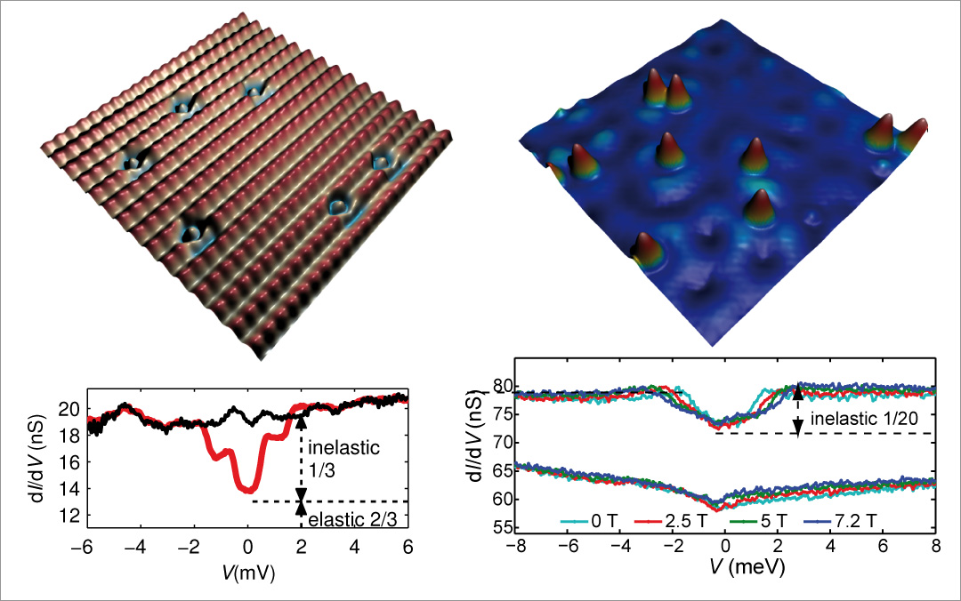
Fig.2: Inelastic scanning tunneling spectroscopy has been performed for Fe atoms adsorbed on different substrates ranging from semiconductors [InSb(110), left panel] to metals [Cu(111), right panels] in order to extract the magnetic moments, anisotropies and excitation lifetimes. As a result of the reduced conduction electron density of states on semiconductors, the atomic spin is more strongly isolated. Consequently, its excitations are sharper, i.e. longer lived, and the tunnel electrons can excite the spin with a much larger efficiency.
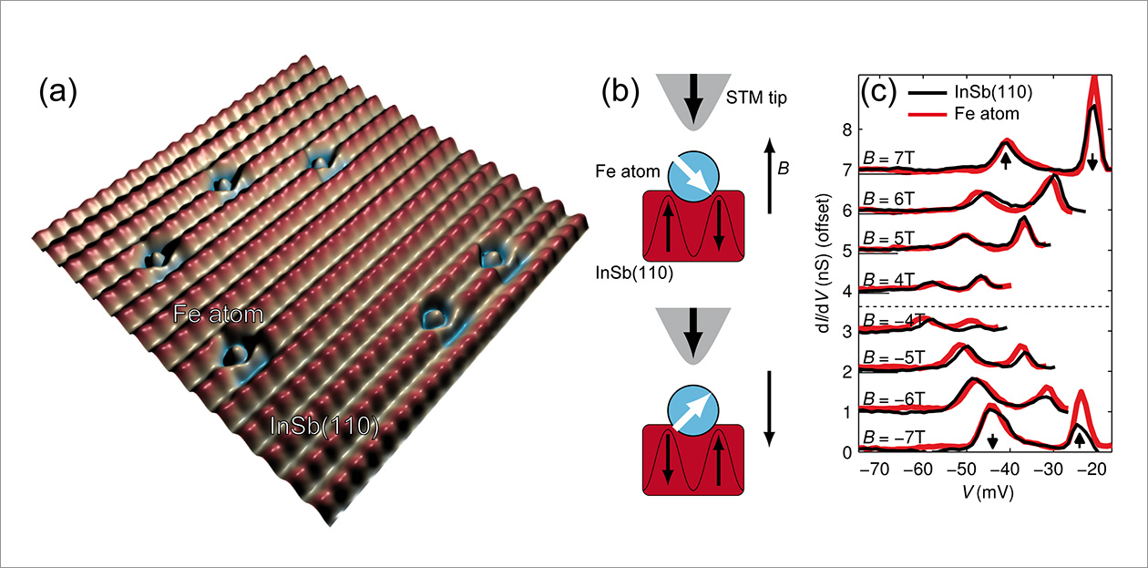
Fig.3: Atomic spins doped into the (110) surface of narrow band gap materials such as Fe / InSb(110) offer the possibility to study the interactions of two-dimensional electron systems with localized atomic spins. We demonstrated that the atomic spins act as valves for spin-polarized electrons tunneling from the Landau Levels within the semiconductor to the tip whose efficiency can exceed that of spin-polarized STM tips.
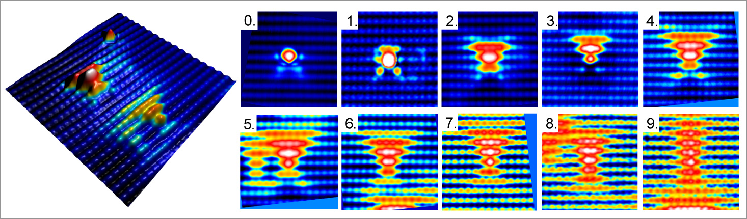
Fig.4: Atomic spins doped into the bulk of three-five semiconductors can be investigated in cross sectional geometry by scanning the natural (110) cleavage plane. Since this surface is free from intrinsic surface states it is possible to investigate the magnetic properties of bulk dopants with a distance of up to ten layers beneath the surface.