Adsorbate induced two dimensional electron gas
To perform STS on a two dimensional electron gas (2DEG) we use the adsorbate induced 2DEG located close to the surface. We characterize it by Photoelectron spectroscopy (UPS). Monitoring valence band features (Fig. 1) allows to measure the band bending as a function of adsorbate coverage (Fig. 2). Close to the Fermi level also the 2DEG itself can be detected (Fig. 3). It shifts down with increasing coverage leading to a tunable carrier density (1011cm-3-range). The strong dispersion of InAs leads to a strong restriction of the 2DEG peak with detection angle (Fig. 4). The subband energies are routinely deduced from the 2DEG peak, but the 2DEG-dispersion has not been resolved. Measurements with higher angular resolution are planned.
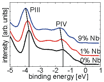 Fig. 1: UPS spectra (hn=13 eV) measured with different Nb-coverages on InAs(110).
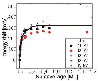 Fig. 2: Band bending as a function of Nb-coverage (line) deduced from energy shift of valence band features (symbols).
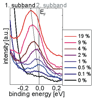 Fig. 3: 2DEG-peak as a function of Nb-coverage. The two subbands calculated from the band bending are indicated.
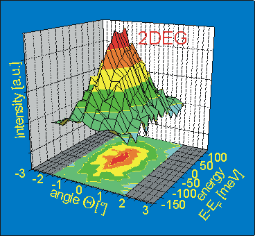 Fig. 4: The 2DEG-peak from InAs(110) covered with 0.5 % Fe