| Introduction to STM | Instrumentation | Projects |
| Gallery | Publications | Team |
GdFe2 islands
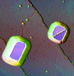 |
Image size: 75 nm x 75 nm Tunneling bias: red: 0.1 V, green: 1.0 V, blue: 2.1 V |
Islands of GdFe2, grown on W(110). Among the islands, the substrate is covered with a monolayer GdFe2. Notice the different colors of the monolayer and the top of the islands! Do you remember what it means? Different electronic structures! (It was explained with the image "Terbium on tungsten") This is the case because the alloy is stressed in the first monolayer. This alone may result in a changed electronic structure, but perhaps a different crystal structure may also play a role. We are still at it.
Go back to the ![]() gallery main page.
gallery main page.
Introduction to STM | Instrumentation | Projects | Gallery | Publications | Team
impressum © copyright 2002 by group R - university of hamburg