| Introduction to STM | Instrumentation | Projects |
| Gallery | Publications | Team |
Terbium on W(110)
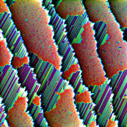 |
Image size: 125 nm x 125 nm Tunneling bias: red: 0.3 V, green: 0.8 V, blue: 1.2 V |
The rare earth metal terbium ( Tb ) was evaporated onto a W(110) single crystal as a thin film. The thickness of the film was less than one single atomic layer. At this low coverage the Tb atoms arrange in parallel lines, so- called "superstructures", visible as stripes. Areas with different distances of the monoatomic stripes are visible. Since the electronic structure of the superstructures depend on this stripe distance, each superstructure exhibits a characteristic color in this three color composite.
This is the main scientific message of these images: different colors mean different electronic structure!
Gadolinium and terbium on W(110)
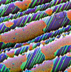 |
Image size: 125 nm x 125 nm Tunneling bias: red: 0.3 V, green: 0.8 V, blue: 1.2 V |
Both rare earth metals gadolinium and terbium arrange in the same kind of chainlike structures on top of the W(110) substrate. What happens if the two metals are alloyed in the coverage range below one monolayer? Is it possible to distiguish between them with the STM? The alloy consisting of Gd and Tb by a ratio of 1:1 looks exactly the same as the pure metals. We found no hint to distinguish between them.
Further reading:
"Atomic and local electronic structure of Gd thin films studied by STM and STS"
R. Pascal, Ch. Zarnitz, M. Bode, and R. Wiesendanger
Phys. Rev. B 56, 3636 (1997)
"STM-study of Gd/W(110) at submonolayer coverages"
R. Pascal, Ch. Zarnitz, M. Bode, R. Wiesendanger
Surf. Sci. 385, L990 (1997)
Go back to the ![]() gallery main page.
gallery main page.
Introduction to STM | Instrumentation | Projects | Gallery | Publications | Team
impressum © copyright 2002 by group R - university of hamburg